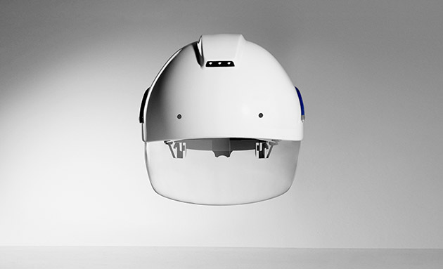
In Los Angeles, a startup called Daqri has designed a different kind of hard hat: an Android-powered one that's capable of augmented reality. As such, it really looks more like a bike helmet than a hard hat, equipped with sensors, cameras and a transparent visor that functions as a head-up display. Unlike Google Glass that was designed with all kinds of consumers in mind, though, this high-tech hat was meant for industrial environments, to be used by engineers or blue-collar workers. It can show instructions and other digital elements superimposed against real-world equipment and objects without having to be manually operated. The hat can also give out early warning signals in case it catches anything that could be dangerous, or perform thorough quality checks on expensive machinery like satellites. If needed, it can pair up with smartwatches, phones and other devices, as well.
Daqri president Andy Lowery told the Wall Street Journalthe company's sparing no expense building the high-tech hat. Couple that with the fact that it's going to need a lot of processing power -- it runs on two Snapdragon processors and will save data on flash cartridges -- and it's easy to guess that it'll be more expensive than other AR headsets. According to Lowery, it'll probably be priced closer to laptops with military capabilities, but we won't know how much for sure until its launch in October.
The biggest target is typically the easiest to hit, and ahead of Apple's big event next week IKEA's taking a good-natured swing at Cupertino. To debut its new 2015 catalog, the Swedish furniture company crafted a video that bears more than a passing resemblance to a TV spot from the iPhone company. Among the highlights of the "bookbook" unveiling? Eternal battery life, no-lag page loads and multiuser support. It's all pretty well done if you ask us. Should you need help passing time until next Tuesday's conference, watching the clip (embedded below) will make the wait about two-and-a-half minutes shorter.
Tipsters have been seemingly eager to shed light on everysinglefacet of Apple's long-rumored smartwatch, but one obvious question hasn't really received a clear answer: will it run third-party apps? If you ask 9to5Mac, the answer is "yes." Its sources claim that the iOS-based wristwear will not only support third-party software, but already has a developer kit to make sure there are plenty of titles ready for the reported launch early next year. There isn't much word about what these apps can do, although they'll supposedly make good use of iOS 8 features like Handoff and widgets to quickly transfer info between the watch and its companion iPhone.
You may even get a peek at what these apps can do at Apple's September 9th event. As with past iOS devices, a handful of developers have supposedly received early access to the programming kit so that they can show off their work at the media shindig. It's not surprising that Apple would create a wearable app platform; Google, Pebble and Samsung already have their own. If true, though, the news might prove comforting to anyone worried that Apple is working on little more than an iPod nano on steroids.
Boeing has a prettystoried history with lasers and now its testing one that can take out UAVs and rockets regardless of where it's installed. A recent trial run of the tech was conducted in Florida under some pretty grueling conditions (heavy fog, rain and wind), to prove that even a lower-powered version of High Energy Laser Mobile Demonstrator -- HEL MD for short -- is capable in a maritime environment. As Boeing tells it, the firm exceeded all of its goals and successfully engaged with some 150 different targetsincluding drones and 60mm mortar shells with its 10 kilowatt laser. Wiredsays that the energy beam is powered by lithium ion batteries, and that the whole setup only requires a diesel-backed generator to keep the wheels of war defense moving. Meaning, running out of fuel, not munitions, is basically the only threat the energy weapon faces.
Perhaps most interesting is the fact that the armament isn't controlled by some arcane set of switches and levers: an Xbox controller and a laptop do the dirty work. The next logical step for the HEL MD? Upping the system's damage with a stronger, 50- or 60-kilowatt laser. Naturally.
Itching to strap on a $1,500 face computer so you can follow directions floating in front of your head? Well, Google just made it a little easier to claim a head-mounted display of your own -- it quietly added Google Glass to the Play Store the other day, and the search giant seems intent on making it sound, well, cool. To hear the Mountain View spinmasters put it, Glass Explorers aren't just the people who need to try tech before the teeming millions. No no, they're "bold and inspiring," folks who "make move and marvel through Glass." This isn't the first time that Google has tried to broaden Glass' reach -- they opened up the Explorer program to all comers in the US back in May, but it insisted at the time that it was still very much a "beta" product. Between then and now we've seen a slightly tweaked version of Glass launch and a few software updates go live -- none of those changes seem terribly earth-shaking, but it sure is interesting to see Google stop treating Glass like a special little flower that isn't ready for public consumption.
Happy Saturday, and welcome to another edition of Feedback Loop! With all the talk of online data breaches this week, we're discussing ways to better protect your data stored in the cloud. After you're done auditing your passwords, let us know what you think of Samsung's new curved Galaxy Note Edge and find out how much fitness trackers are helping your fellow readers. Make yourself comfy and join us after the break for some in-depth tech talk.
HOW ARE YOU KEEPING YOURSELF SAFE ONLINE?
In light of the recent iCloud security issue, I'm curious to find out how you protect yourself online. Obviously, strong credentials are the way to go, but are you using password managers? Do you go the extra mile by also enabling two-factor authentication? Come join the discussion and share your tips for staying safe in the cloud.
WHO IS THE GALAXY NOTE EDGE FOR?
Samsung likes to get a little crazy with mobile devices, and at IFA this week, the Galaxy Note Edge captured everyone's attention. The curved screen has TgD asking just who is the Note Edge made for? Check out Brad's hands-on first, and then head to the forumsto share your own theories.
FACEBOOK MESSENGER: GIVE IN, OR SAY GOODBYE
Decoupling apps is all the rage right now. Foursquare kicked things off with Swarm and Facebook finally spun out Messenger for good. John isn't thrilled with this move; he doesn't understand why we need multiple apps for a single service. Is this the final strawfor Facebook on your phone?
ARE FITNESS TRACKERS IMPROVING YOUR HEALTH?
Even though fitness analytics are showing up in phones and smartwatches, the dedicated tracker market is still kicking. They're coming in the form of bracelets, watches (the non-smart kind) and more. The age-old question still remains though: Do they actually work? A few of our readers have already shared their success stories, so come join thediscussion and let us know if all that data-tracking is working for you.
It was going to be either me or my male colleague. That's a lie: It was absolutely going to be me. It was my last day at IFA, Europe's biggest technology show, and Brad Molen and I were sitting inside a sparsely decorated smart home that Panasonic had built in the middle of the demo area. Panasonic needed a volunteer to sit in front of its prototypical smart mirror, which applies digital "makeup" so you can sample new looks. I exchanged a look with Brad, imagining his bearded cheeks with blush on them. Then I sat down and agreed to let a machine tell me everything that was wrong with my face.
Embarrassingly enough, this isn't even the first time I've tested such a product for Engadget. Back at CES, if you recall, I got hands-on with a modded Windows PC that used a Kinect sensor to apply makeup and give people nose jobs. If that's all Panasonic's mirror did, I would have walked away, my dignity intact. But this thing is a little more sophisticated. With the help of sensors and facial recognition software (the same kind as Panasonic's cameras), it creates an enlarged, hologram-like image of your face, and then diagnoses your weak areas -- wrinkles, smile lines, blemishes, et cetera.
When it's done, it makes custom recommendations based on your skin condition. In my case, the mirror zeroed in on the dark circles under my eyes, marking the area with a series of blue lines. I was jetlagged, exhausted and operating on very little sleep. "Get this girl some concealer!" it may as well have said. Then it offered to sell me anti-aging products and have me download a juice recipe. Well played, machine. Well played.
From there, you can do all sorts of things to your eyebrows, lips, cheeks and eyebrows, just as you'd expect. For the purposes of this demo, the presenter was using a remote, but it's also capable of voice commands, including "Mirror off." In addition, the mirror could in theory sync with your calendar, and recommend entire looks for different occasions. A first date after work? Meeting with clients? Spending the day at a trade show? (J/k: The answer there is "no makeup.") Of course, I say "in theory" for a reason: Not only is this a prototype, but it isn't necessarily destined for your home, either. Instead, a Panasonic rep told me, the mirror is really intended for places like salons and department stores. Which is just as well: Only a professional could tell me when a space-alien look is called for.
Once, Silicon Valley was all about garages. It seemed if you put a couple of smart engineers together in a garage, magical things happened.
These days, it’s about incubators; these sometimes-big operations host as many as 80 or more tiny companies whose founders are busily developing prototypes and fine-tuning business plans. Incubators are often funded by investors who take a little piece of each of the companies they incubate.
Garages have an important advantage over incubators—if your company is in your garage, it’s easy to work day and night, or any time you get the impulse. Get a great idea in the shower? You can start testing it out in about as long as it takes you to towel off.
Companies in incubators, though, have an advantage of their own—the presence of other smart engineers to act as inspirations, sounding boards, and sometimes collaborators.
It appears that Scott Hassan—who worked with Google founders Larry Page and Sergey Brin to develop an early version of the company's technology, sold a company to Yahoo for $413 million (some of which he invested in Google), and founded robotic research lab Willow Garage—is going to try to combine the advantages of both the garage and the incubator. Hassan, it came out last week, is behind a large real estate development in Menlo Park, Calif. He reportedly plans to create an incubator village with 18,500 square meters of workspace and another 18,500 square meters of living space on a 30,000 square meter site.
Hassan has room on his plate for something new. He essentially shut down Willow Garage last year, after seven years of operation. Hassan has been involved with Willow Garage spinoff, Suitable Technologies. (Another spin-off company, Unbounded Robotics, shut down this summer.) But it turns out he had another project in the works at least since last year.
Hassan doesn’t talk to the press that often, and didn’t respond to my request to discuss his plans for the Menlo Park incubator village. Last week, Bob Burke, a principal at Greenheart Land Companies, told the Palo Alto Daily Post that Hassan plans to create a space for young tech entrepreneurs to work and live, one that is close to downtown restaurants and transit. Beyond that, Burke gave little detail. (The article is not yet available online.)
Hassan’s incubator village isn’t exactly a done deal. Last November, the proposal submitted to the City of Menlo Park by Greenheart (Hassan’s involvement had yet to be revealed) generated some pushback. A group of residents called Save Menlo Park organized to limit the amount of office space on the project (and other large developments) to 9300 square meters; they succeeded in placing an initiative that would set such a limit on the upcoming November ballot. Arguments in favor of what is called Measure M surround concerns over commute traffic generated by workers at the complex, leading to rush-hour gridlock on busy El Camino Real and therefore more traffic cutting through neighborhoods.
These arguments were written up when the project was simply described as a mix of office and residential space. The "incubator village" concept, however, eliminates the commute issue; in a true incubator village, residents would walk to work, and only use cars in off hours. With that concept and Hassan's involvement on the table, I asked one of the residents behind Save Menlo Park if he now is less worried about the proposed development. He told me that thinks Hassan's incubator would be interesting—built somewhere else—because he doesn’t see it as cutting traffic, believing both the apartments and the office space will go to the highest bidders, with no real link between the two.
Indeed, I am curious about how Hassan plans to get entrepreneurs to live as well as work on the site, and if such a program is sustainable—when companies move, will the engineers have to move too? Will he offer free rentals? Subsidized housing? However, I am more optimistic than the Save Menlo backer that Hassan will do something more interesting with this project than just make money. For one, this isn’t the first time he’s tried to make it easy for engineers to live close to work—in its day, Willow Garage bought a few houses near its Menlo Park offices and set them up as residences for the company’s interns. For another, Hassan has shown that he looks at buildings as places to generate companies, not rental income. According toBusiness Week, Willow Garage started when Hassan “snagged some prime office space in Menlo Park.” He then tapped Steve Cousins, a former Xerox Parc and IBM research lab manager, as CEO and simply told him to fill the building with interesting stuff, with the mantra being: “Impact first and return on capital second.”
So it’s possible that’s what Hassan will do in Menlo Park—focus on impact first and return on capital second. That is, if his project is not blocked, he’s likely to get it built and then get someone to fill it with “interesting stuff.” Will it be interesting enough to make tech workers used to San Francisco’s restaurants and nightlife want to get off the bus and live where they work? Stay tuned.
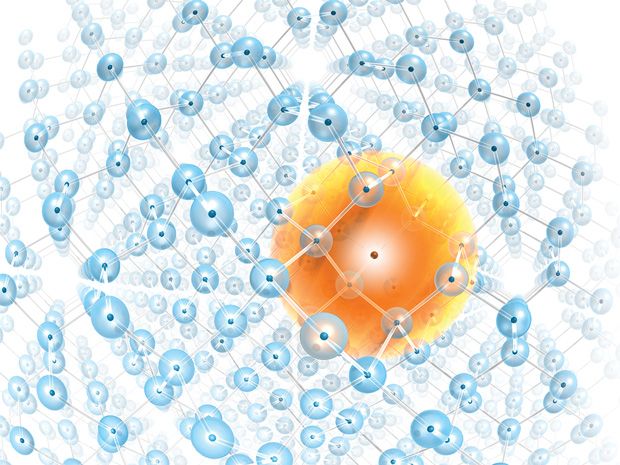
At Display Week 2014, high-efficiency quantum dots sharpen colors
Dotty Displays: The Kindle Fire HDX is one of the first consumer devices to use displays with quantum dots.
Rumpelstiltskin had the admirable ability to convert low-cost straw into valuable gold. Today, display manufacturers are starting to reap the benefits of their own photonic alchemy, converting the light from cheap sources into the precise wavelengths needed for more efficient displays that can show sharper colors.
This magic is accomplished using what are known as quantum dots. These are semiconductor nanocrystals that exhibit a range of unusual electrical and optical properties, but for decades they were largely confined to research laboratories. Now, quantum dots are being used in mass-produced displays for the consumer market, including such items as Sony flat-screen televisions and Amazon.com’s Kindle Fire HDX e-reader. And the field is still rapidly growing and evolving. At the Display Week 2014 conference of the Society for Information Display this past June in San Diego, quantum dots were a hot topic, both in the exhibit hall and in presented papers; the symposium schedule included three separate sessions dedicated to the subject.
Quantum dots have many interesting properties, but when it comes to displays the most important thing about them is that they can absorb light of short (blue) wavelengths and then emit it as light of longer (red and green) wavelengths. This might sound a lot like traditional phosphor materials, which made the cathode ray tube (CRT) possible by converting a beam of electrons into visible colors. The difference is that quantum dots produce much more precise emissions. A good phosphor has an emission range of about 50 nanometers, while a typical quantum dot’s range is about half that. Just where on the spectrum that range is can be carefully controlled by varying the size of the particles; the larger the particle, the longer the wavelength of the emissions will be. The peak emissions of the quantum dot can be tuned to within 1 nm. This gives excellent control over the color output of the display.
And conveniently, while quantum dots can emit a very narrow range of wavelengths, the light source they are converting from can have a broader range and the light will still be converted with an efficiency of more than 95 percent. All this helps make quantum dots much less wasteful than traditional backlight approaches, where a lot of light is lost in a color-filter layer that screens out undesirable wavelengths. With more of the light getting to the viewer, the result is a display that is brighter without upping power consumption.
Color reproduction has become an increasingly important topic in the display industry. For years, CRT quality was considered “good enough,” even though the typical CRT display was able to show only about 70 to 75 percent of the gamut of colors specified in the National Television System Committee (NTSC) color standard.
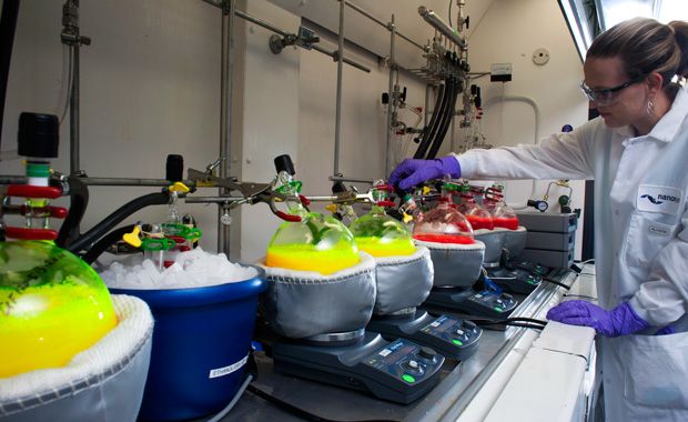
Photo: 3MQuantum Colors: A Nanosys technician works with batches of materials infused with quantum dots of different sizes, resulting in the emission of different colors.
Advances in color displays—first with LCDs and more recently with OLEDs—have made it possible to exceed the boundaries of the NTSC standard. Consequently, expanded color-gamut standards have come into play, the most recent of which is ITU-R Recommendation BT.2020, created by theInternational Telecommunication Union to measure the color space used by next-generation ultrahigh-definition (UHD) televisions. Some prototype quantum-dot-based displays can already reproduce 95 percent of the color gamut specified by Rec. 2020.
Two companies have taken the lead in commercializing quantum-dot technology. QD Vision is the company behind Sony’s Triluminus technology, and Nanosys has partnered with 3M Co. to create Quantum Dot Enhancement Film (QDEF), a light-processing film.
The QD Vision approach adds quantum dots to strips of blue LED edge lights around an LCD panel. Some of this light is converted to red and green, which is mixed by a light guide to create a high-quality white backlight for the LCD panel’s color subpixels. The Nanosys/3M approach places the QDEF film over the back of the panel, and then a blue LED backlight is applied (typically through edge lighting and a light guide). Some of the blue light is converted in the film layer to red and green light before reaching a subpixel.
A new, third, approach is being developed by a number of researchers. This involves putting the quantum dots directly on the blue LED chip. This can simplify the optical and light-management requirements, but it subjects the quantum-dot material to higher operating temperatures that can decrease performance.
As you might expect, a technology that simultaneously increases color performance and power efficiency is attracting a lot of commercial interest. New products continue to appear; at Display Week, Asus announced theZenbook NX500, the first high-gamut 4K-resolution notebook computer, which uses 3M’s QDEF quantum-dot film.
Market research firm IHS projects that the market for displays that incorporate quantum dots will grow from about US $10 million in 2013 to $200 million by 2020. And according to Touch Display Research, the quantum-dot materials market is projected to grow from $70 million in 2013 to $9.6 billion in 2023.
One problem with quantum dots is that they require cadmium, which is on the European Union’s Restriction of Hazardous Substances (RoHS) regulation list. However, researchers are working on creating cadmium-free quantum dots. Dow Electronic Materials has licensed technology from Nanoco Group to produce such materials; commercial production is slated to start this year.
In any case, it appears that quantum dots will play an important role in the new UHD television market, while helping LCD panels compete more effectively with OLEDs for a broader range of devices. The end result will be that you’ll see colors on the screen that until now you’ve seen only in real life.
Objects can go undetected by sight, sound, or heat with these tricks
In 2006, scientists at Duke University captured the world’s imagination by announcing they had created an invisibility cloak. It could hide an object only from a particular wavelength in the microwave region, and only when viewed from certain directions, but it sparked waves of research along with countless cracks about boy wizards and Romulan warbirds. You still can’t hide a spaceship, but that hasn’t stopped scientists from coming up with new and strange ways to make small objects undetectable, and the past few months have produced particularly unusual innovations.
Invisibility is accomplished using metamaterials, which feature structures that are substantially smaller than the wavelengths of light. For instance, an early metamaterial, described in 2008 by Xiang Zhang, a professor of mechanical engineering at the University of California, Berkeley, consisted of 30-nanometer-thick layers of silver interwoven in a fishnet pattern with 50-nm-thick layers of magnesium fluoride. The right arrangement of structures gives the material a negative index of refraction, allowing it to bend light of a particular wavelength in directions it would not normally bend. With careful engineering, the idea goes, you could route the light around an object and let it continue on as if the object weren’t there.
Since the original work, researchers have found methods to cover wider bands of wavelengths and make objects invisible from a wider field of view. They’ve even developed cloaks to hide things at visible wavelengths, although the hidden objects tend to be just a few millimeters wide. Zhang says that in theory it’s possible to build cloaks for any sort of wave, including sound waves and heat waves. In practice, while there have been plenty of advancements in the last half dozen years, there are still a lot of problems to be solved. “You can make cloaks. The question is, can you scale them up?” Zhang says. He believes invisibility will eventually be possible, but, he says, “I wouldn’t say how long it will take. It’s not an easy task.” Here are three new ways that researchers are using to make objects invisible.
Photo: University of Buffalo
1. Hiding in a Hole
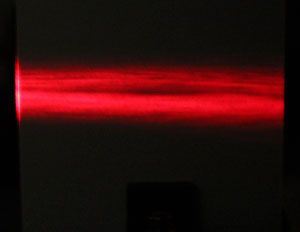
While most approaches to making an object invisible entail building something to hide the object, Natalia Litchinitser, associate professor of electrical engineering at the State University of New York at Buffalo, proposes structuring the light itself in such a way that it misses the object and then continues on unchanged. In her experiment, she shot a beam of light from a laser and expanded it so it had a diameter of 10 millimeters. Then she passed it through a spiral phase plate, which wound the beam into a helical structure, like the coils of a spring. She passed the beam over a thin metal rod, as if she were slipping the spring over a nail, and then through another phase plate, which returned the beam to its original shape. Because the rod rested in the empty space in the middle of the beam, it wasn’t visible. Of course, the object to be hidden has to fit into the relatively small hole in the light beam, and it works only if the beam passes in the right direction. But Litchinitser says her approach might be combined with more conventional metamaterial approaches to improve the performance of both.
Photo: Duke University
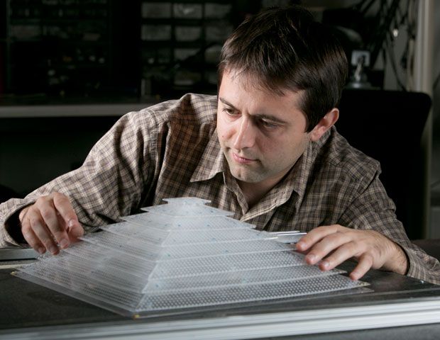
2. Cone of Silence
Instead of light, Steven Cummer, a professor of electrical and computer engineering at Duke University, designs his metamaterials to manipulate sound waves. Sonar “sees” an object by measuring distortions in the reflected sound waves that bounce off it. To hide an object from sonar, the metamaterial must be designed so that sound bounces off it in the same pattern it would if it were being reflected by the surface beneath it. In his experiment, Cummer wanted to hide a small plastic pyramid, so he built a cloaking pyramid to cover it. He built this undetectable pyramid out of air-filled cubes of acrylic and used a laser cutter to perforate acrylic plates within each cube with 850-micrometer-wide holes. Each unit of this periodic structure is about 1/20th the size of the wavelength of the 3-kilohertz sound used by the detector. The researchers pinged their cloak from many different angles to make sure it worked in 3-D space. Though the experimental results weren’t perfect, the cloak did manage to mostly mask the plastic pyramid beneath it.
Photo: National University of Singapore
3. Hidden Heat
One way to camouflage an object is to hide its heat signature. Cheng-WeiQiu, assistant professor of electrical and computer engineering, and his colleagues at the National University of Singapore have come up with athermal cloak that masks how heat scatters off an object. They use a bilayer cloak with different levels of conductivity in each layer. The inner layer in this case is silicone, which is an insulator. The outer layer is copper, which of course is highly conductive. The combination causes heat to flow differently around the hidden object than it normally would. Instead of producing one thermal signature where the object is, there are now scattered signatures at different locations. To complete the illusion, Qiu places other objects at the locations of these “ghost” heat signatures, so the scene appears ordinary. Qiu calls the hidden object—really a copper cylinder—a “man” and the ghost objects, which are insulators, “women.” With the cloak in place, the man vanishes among the women.
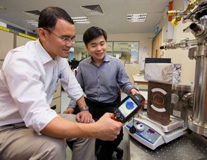
Silicon has become a leading contender in the hunt for a practical, scalable quantum bit
Grand engineering challenges often require an epic level of patience. That’s certainly true for quantum computing. For a good 20 years now, we’ve known that quantum computers could, in principle, be staggeringly powerful, taking just a few minutes to work out problems that would take an ordinary computer longer than the age of the universe to solve. But the effort to build such machines has barely crossed the starting line. In fact, we’re still trying to identify the best materials for the job.
Today, the leading contenders are all quite exotic: There are superconducting circuits printed from materials such as aluminum and cooled to one-hundredth of a degree above absolute zero, floating ions that are made to hover above chips and are interrogated with lasers, and atoms such as nitrogen trapped in diamond matrices.
These have been used to create modest demonstration systems that employ fewer than a dozen quantum bits to factor small numbers or simulate some of the behaviors of solid-state materials. But nowadays those exotic quantum-processing elements are facing competition from a decidedly mundane material: good old silicon.
Silicon had a fairly slow start as a potential quantum-computing material, but a flurry of recent results has transformed it into a leading contender. Last year, for example, a team based at Simon Fraser University in Burnaby, B.C., Canada, along with researchers in our group at University College London, showed that it’s possible to maintain the state of quantum bits in silicon for a record 39 minutes at room temperature and 3 hours at low temperature. These are eternities by quantum-computing standards—the longevity of other systems is often measured in milliseconds or less—and it’s exactly the kind of stability we need to begin building general-purpose quantum computers on scales large enough to outstrip the capabilities of conventional machines.
As fans of silicon, we are deeply heartened by this news. For 50 years, silicon has enabled steady, rapid progress in conventional computing. That era of steady gains may be coming to a close. But when it comes to building quantum computers, the material’s prospects are only getting brighter. Silicon may prove to have a second act that is at least as dazzling as its first.
What is a quantum computer? Simply put, it’s a system that can store and process information according to the laws of quantum mechanics. In practice, that means the basic computational components—not to mention the way they operate—differ greatly from those we associate with classical forms of computing.
For example, as bizarre as it sounds, in the quantum world an object can exist in two different states simultaneously—a phenomenon known as superposition. This means that unlike an ordinary bit, a quantum bit (or qubit) can be placed in a complex state where it is both 0 and 1 at the same time. It’s only when you measure the value of the qubit that it is forced to take on one of those two values.
When a quantum computer performs logical operations, it does so on all possible combinations of qubit states at the same time. This massively parallel approach is often cited as the reason that quantum computers would be very fast. The catch is that often you’re interested in only a subset of those calculations. Measuring the final state of a quantum machine will give you just one answer, at random, that may or may not be the desired solution. The art of writing useful quantum algorithms lies in getting the undesired answers to cancel out so that you are left with a clear solution to your problem.
The only company selling something billed as a “quantum computing” machine is the start-up D-Wave Systems, also based in Burnaby. D-Wave’s approach is a bit of a departure from what researchers typically have in mind when they talk about quantum computing, and there is active debate over the quantum-mechanical nature and the potential of its machines (more on that in a moment).
The quarry for many of us is auniversal quantum computer, one capable of running any quantum or classical algorithm. Such a computer won’t be faster than classical computers across the board. But there are certain applications for which it could prove exceedingly useful. One that quickly caught the eye of intelligence agencies is the ability to factor large numbers exponentially faster than the best classical algorithms can. This would make short work of cryptographic codes that are effectively uncrackable by today’s machines. Another promising niche is simulating the behavior of quantum-mechanical systems, such as molecules, at high speed and with great fidelity. This capability could be a big boon for the development of new drugs and materials.
To build a universal quantum computer capable of running these and other quantum algorithms, the first thing you’d need is the basic computing element: the qubit. In principle, nearly any object that behaves according to the laws of quantum physics and can be placed in a superposition of states could be used to make a qubit.
Since quantum behavior is typically most evident at small scales, most natural qubits are tiny objects such as electrons, single atomic nuclei, or photons. Any property that could take on two values, such as the polarization of light or the presence or absence of an electron in a certain spot, could be used to encode quantum information. One of the more practical options is spin. Spin is a rather abstruse property: It reflects a particle’s angular momentum—even though no physical rotation is occurring—and it also reflects the direction of an object’s intrinsic magnetism. In both electrons and atomic nuclei, spin can be made to point up or down so as to represent a 1 or a 0, or it can exist in a superposition of both states.
It’s also possible to make macroscopic qubits out of artificial structures—if they can be cooled to the point where quantum behavior kicks in. One popular structure is the flux qubit, which is made of a current-carrying loop of superconducting wire. These qubits, which can measure in the micrometers, are quantum weirdness writ large: When the state of a flux qubit is in superposition, the current flows in both directions around the loop at the same time.
D-Wave uses qubits based on superconducting loops, although these qubits are wired together to make a computer that operates differently from a universal quantum computer. The company employs an approach called adiabatic quantum computing, in which qubits are set up in an initial state that then “relaxes” into an optimal configuration. Although the approach could potentially be used to speedily solve certain optimization problems, D-Wave’s computers can’t be used to implement an arbitrary algorithm. And the quantum-computing community is still actively debating the extent to which D-Wave’s hardware behaves in a quantum-mechanical fashion and whether it will be able to offer any advantage over systems using the best classical algorithms.
Although large-scale universal quantum computers are still a long way off, we are already getting a good sense of how we’d make one. There are several approaches. The most straightforward one employs a model of computation known as the gate model. It uses a series of “universal gates” to wire up groups of qubits so that they can be made to interact on demand. Unlike conventional chips with hardwired logic circuitry, these gates can be used to configure and reconfigure the relationships between qubits to create different logic operations. Some, such as XOR and NOT, may be familiar, but many won’t be, since they’re performed in a complex space where a quantum state in superposition can take on any one of a continuous range of values. But the basic flow of computation is much the same: The logic gates control how information flows, and the states of the qubits change as the program runs. The result is then read out by observing the system.
Another, more exotic idea, called the cluster-state model, operates differently. Here, computation is performed by the act of observation alone. You begin by first “entangling” every qubit with its neighbors up front. Entanglement is a quantum-mechanical phenomenon in which two or more particles—electrons, for example—share a quantum state and measuring one particle will influence the behavior of an entangled partner. In the cluster-state approach, the program is actually run by measuring the qubits in a particular order, along particular directions. Some measurements carve out a network of qubits to define the computation, while other measurements drive the information forward through this network. The net result of all these measurements taken together gives the final answer.
For either approach to work, you must find a way to ensure that qubits stay stable long enough for you to perform your computation. By itself, that’s a pretty tall order. Quantum-mechanical states are delicate things, and they can be easily disrupted by small fluctuations in temperature or stray electromagnetic fields. This can lead to significant errors or even quash a calculation in midstream.
On top of all this, if you are to do useful calculations, you must also find a way to scale up your system to hundreds or thousands of qubits. Such scaling wouldn’t have been feasible in the mid-1990s, when the first qubits were made from trapped atoms and ions. Creating even a single qubit was a delicate operation that required elaborate methods and a roomful of equipment at high vacuum. But this has changed in the last few years; now there’s a range of quantum-computing candidates that are proving easier to scale up [see “Quantum Contenders”].
Among these, silicon-based qubits are our favorites. They can be manufactured using conventional semiconductor techniques and promise to be exceptionally stable and compact.
It turns out there are a couple of different ways to make qubits out of silicon. We’ll start with the one that took the early lead: using atoms that have been intentionally placed within silicon.
If this approach sounds familiar, it’s because the semiconductor industry already uses impurities to tune the electronic properties of silicon to make devices such as diodes and transistors. In a process called doping, an atom from a neighboring column of the periodic table is added to silicon, either lending an electron to the surrounding material (acting as a “donor”) or extracting an electron from it (acting as an “acceptor”).
Such dopants alter the overall electronic properties of silicon, but only at temperatures above –220 °C or so (50 degrees above absolute zero). Below that threshold, electrons from donor atoms no longer have enough thermal energy to resist the tug of the positively charged atoms they came from and so return.
This phenomenon, known as carrier freeze-out, describes the point at which most conventional silicon devices stop working. But in 1998, physicist Bruce Kane, now at the University of Maryland, College Park, pointed out that freeze-out could be quite useful for quantum computing. It creates a collection of electrically neutral, relatively isolated atoms that are all fixed in place—a set of naturally stable quantum systems for storing information.
In this setup, information can be stored in two ways: It can be encoded in the spin state of the donor atom’s nucleus or of its outermost electron. The state of a particle’s spin is very sensitive to changing magnetic fields as well as interactions with nearby particles. Particularly problematic are the spins of other atomic nuclei in the vicinity, which can flip at random, scrambling the state of electron-spin qubits in the material.
But it turns out that these spins are not too much trouble for silicon. Only one of its isotopes—silicon-29—has a nucleus with nonzero spin, and it makes up only 5 percent of the atoms in naturally occurring silicon. As a result, nuclear spin flips are rare, and donor electron spins have a reasonably long lifetime by quantum standards. The spin state of the outer electron of a phosphorus donor, for example, can remain in superposition as long as 0.3 millisecond at 8 kelvins before it’s disrupted.
That’s about the bare minimum for what we’d need for a quantum computer. To compensate for the corruption of a quantum state—and to keep quantum information intact indefinitely—additional long-lived qubits dedicated to identifying and correcting errors must be incorporated for every qubit dedicated to computation. One of the most straightforward ways to do this is to add redundancy, so that each computational qubit actually consists of a group of qubits. Over time, the information in some of these will be corrupted, but the group can be periodically reset to whatever state the majority is in without disturbing this state. If there is enough redundancy and the error rate is below the threshold for “fault tolerance,” the information can be maintained long enough to perform a calculation.
If a qubit lasts for 0.3 ms on average and can be manipulated in 10 nanoseconds using microwave radiation, it means that on average 30,000 gate operations can be performed on it before the qubit state decays. Fault tolerance thresholds vary, but that’s not a very high number. It would mean that a quantum computer would spend nearly all its time correcting the states of qubits and their clones, leaving it little time to run meaningful computations. To reduce the overhead associated with error correction and create a more compact and efficient quantum computer, we must find a way to extend qubit lifetimes.
One way to do that is to use silicon that doesn’t contain any silicon-29 at all. Such silicon is hard to come by. But about 10 years ago, the Avogadro Project, an international collaboration working on the redefinition of the kilogram, happened to be making some in order to create pristine balls of silicon-28 for their measurements. Using a series of centrifuges in Russia, the team acquired silicon that was some 99.995 percent silicon-28 by number, making it one of the purest materials ever produced. A group at Princeton University obtained some of the leftover material and, in 2012, after some careful experimental work, reported donor electron spin lifetimes of more than a second at 1.8 kelvins—a world record for an electron spin in any material. This really showed silicon’s true potential and established it as a serious contender.
Our group has since shown that the spins of some donor atoms—bismuth in particular—can be tuned with an external magnetic field to certain “sweet spots” that are inherently insensitive to magnetic fluctuations. With bismuth, we found that the electron spin states can last for as long as 3 seconds in enriched silicon-28 at even higher temperatures. Crucially, we found lifetimes as high as 0.1 second in natural silicon, which means we should be able to achieve relatively long qubit lifetimes without having to seek out special batches of isotopically pure material.
These sorts of lifetimes are great for electrons, but they pale in comparison to what can be achieved with atomic nuclei. Recent measurements led by a team at Simon Fraser University have shown that the nuclear spin of phosphorus donor atoms can last as long as 3 minutes in silicon at low temperature. Because the nuclear spin interacts with the environment primarily through its electrons, this lifetime increases to 3 hours if the phosphorus’s outermost electron is removed.
Nuclear spins tend to keep their quantum states longer than electron spins because they are magnetically weaker, and thus their interaction with the environment is not as strong. But this stability comes at a price, because it also makes them harder to manipulate. As a result, we expect that quantum computers built from donor atoms might use both nuclei and electrons. Easier-to-manipulate electron spins could be used for computation, and more stable nuclear spins could be deployed as memory elements, to store information in a quantum state between calculations.
The record spin lifetimes mentioned so far were based on measuring ensembles of donors all at once. But a major challenge remained: How do you manipulate and measure the state of just one donor qubit at a time, especially in the presence of thousands or millions of others in a small space? Up until just a few years ago, it wasn’t clear how this could be done. But in 2010, after a decade of intense research and development, a team led by Andrea Morello and Andrew Dzurak at the University of New South Wales, in Sydney, showed it’s possible to control and read out the spin state of a single donor atom’s electron. To do this, they placed a phosphorus donor in close proximity to a device called a metal-oxide-semiconductor single-electron transistor (SET), applied a moderate magnetic field, and lowered the temperature. An electron with spin aligned against the magnetic field has more energy than one whose spin aligns with the field, and this extra energy is enough to eject the electron from the donor atom. Because SETs are extremely sensitive to the charge state of the surrounding environment, this ionization of a dopant atom alters the current of the SET. Since then, the work has been extended to the control and readout of single nuclear spin states as well.
SETs could be one of the key building blocks we need to make functional qubits. But there are still some major obstacles to building a practical quantum computer with this approach. At the moment, an SET must operate at very low temperatures—a fraction of a degree above absolute zero—to be sensitive enough to read a qubit. And while we can use a single device to read out one qubit, we don’t yet have a detailed blueprint for scaling up to large arrays that integrate many such devices on a chip.
There is another approach to making silicon-based qubits that could prove easier to scale. This idea, which emerged from work by physicists David DiVincenzo and Daniel Loss, would make qubits from single electrons trapped inside quantum dots.
In a quantum dot, electrons can be confined so tightly that they’re forced to occupy discrete energy levels, just as they would around an atom. As in a frozen-out donor atom, the spin state of a confined electron can be used as the basis for a qubit.
The basic recipe for building such “artificial atoms” calls for creating an abrupt interface between two different materials. With the right choice of materials, electrons can be made to accumulate in the plane of the interface, where there is lower potential energy. To further restrict an electron from wandering around in the plane, metal gates placed on the surface can repel it so it’s driven to a particular spot where it doesn’t have enough energy to escape.
Large uniform arrays of silicon quantum dots should be easier to fabricate than arrays of donor qubits, because the qubits and any devices needed to connect them or read their states could be made using today’s chipmaking processes.
But this approach to building qubits isn’t quite as far along as the silicon donor work. That’s largely because when the idea for quantum-dot qubits was proposed in 1998, gallium arsenide/gallium aluminum arsenide (GaAs/GaAlAs) heterostructures were the material of choice. The electronic structure of GaAs makes it easy to confine an electron: It can be done in a device that’s about 200 nanometers wide, as opposed to 20 nm in silicon. But although GaAs qubits are easier to make, they’re far from ideal. As it happens, all isotopes of gallium and arsenic possess a nuclear spin. As a result, an electron trapped in a GaAs quantum dot must interact with hundreds of thousands of Ga and As nuclear spins. These interactions cause the spin state of the electron to quickly become scrambled.
Silicon, with only one isotope that carries nuclear spin, promises quantum-dot qubit lifetimes that are more than a hundred times as long as in GaAs, ultimately approaching seconds. But the material faces challenges of its own. If you model a silicon quantum dot on existing MOS transistor technology, you must trap an electron at the interface between silicon and oxide, and those interfaces have a fairly high number of flaws. These create shallow potential wells that electrons can tunnel between, adding noise to the device and trapping electrons where you don’t want them to be trapped. Even with the decades of experience gained from MOS technology development, building MOS-like quantum dots that trap precisely one electron inside has proven to be a difficult task, a feat that was demonstrated only a few years ago.
As a result, much recent success has been achieved with quantum dots that mix silicon with other materials. Silicon-germanium heterostructures, which create quantum wells by sandwiching silicon between alloys of silicon and germanium and have much lower defect densities at the interface than MOS structures, have been among the front-runners. Earlier this year, for example, a team based at the Kavli Institute of Nanoscience Delft, in the Netherlands, reported that they had made silicon-germanium dots capable of retaining quantum states for 40 microseconds. But MOS isn’t out of the running. Just a few months ago, Andrew Dzurak’s group at the University of New South Wales reported preliminary results suggesting that it had overcome issues of defects at the oxide interfaces. This allowed the group to make MOS quantum dots in isotopically pure silicon-28 with qubit lifetimes of more than a millisecond, which should be long enough for error correction to take up the slack.
As quantum-computing researchers working with silicon, we are in a unique position. We have two possible systems—donors and quantum dots—that could potentially be used to make quantum computers.
Which one will win out? Silicon donor systems—both electron and nuclear spins—have the advantage when it comes to spin lifetime. But embedded as they are in a matrix of silicon, donor atoms will be hard to connect, or entangle, in a well-controlled way, which is one of the key capabilities needed to carry out quantum computations. We might be able to place qubits fairly close together, so that the donor electrons overlap or the donor nuclei can interact magnetically. Or we could envision building a “bus” that allows microwave photons to act as couriers. It will be hard to place donor atoms precisely enough for either of these approaches to work well on large scales, although recent work by Michelle Simmons at the University of New South Wales has shown it is possible to use scanning tunneling microscope tips to place dopants on silicon surfaces with atomic precision.
Silicon quantum dots, which are built with small electrodes that span 20 to 40 nm, should be much easier to build uniformly into large arrays. We can take advantage of the same lithographic techniques used in the chip industry to fabricate the devices as well as the electrodes and other components that would be responsible for shuttling electrons around so they can interact with other qubits.
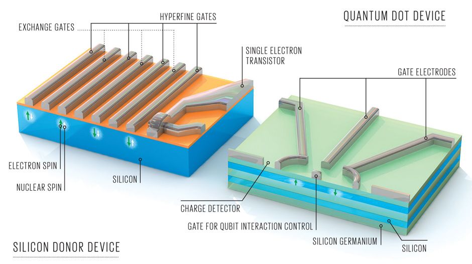
Illustration: Bryan Christie DesignIn Silico Qubits: There are two potential ways to build a quantum computer from silicon. Donor nuclei, embedded in silicon crystals, and their outermost electrons might be read using single electron transistors [left]. Two sets of gates could be used to set the states of the qubits (hyperfine gates) and control their interactions (exchange gates). Potentially easier to fabricate on large scales will be quantum dots [right], which use electrodes to trap individual electrons in thin layers of material. Illustrated here is one device concept, which employs layers of silicon and silicon germanium.
Given these different strengths, it’s not hard to envision a quantum computer that would use both types of qubits. Quantum dots, which would be easier to fabricate and connect, could be used to make the logic side of the machine. Once a part of the computation is completed, the electron could be nudged toward a donor electron sitting nearby to transfer the result to memory in the donor nucleus.
Of course, silicon must also compete with a range of other exciting potential quantum-computing systems. Just as today’s computers use a mix of silicon, magnetic materials, and optical fibers to compute, store, and communicate, it’s quite possible that tomorrow’s quantum computers will use a mix of very different materials.
We still have a long way to go before silicon can be considered to be on an equal footing with other quantum-computing systems. But this isn’t the first time silicon has played catch-up. After all, lead sulfide and germanium were used to make semiconducting devices before high-purity silicon and CMOS technology came along. So far, we have every reason to think that silicon will survive the next big computational leap, from the classical to the quantum age.
This article originally appeared in print as “Silicon’s Second Act.”


-1398183503547.jpg)